Apple M2 Die Shot and Architecture Analysis – Big Cost Increase And A15 Based IP
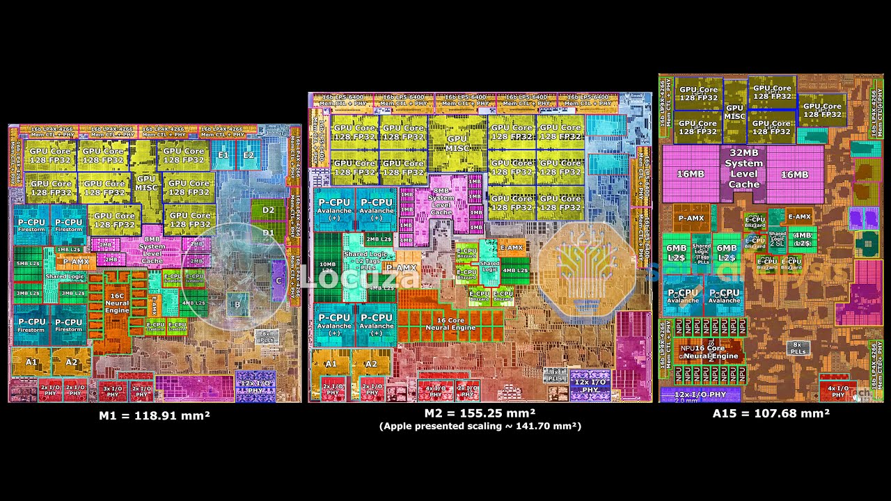
Dylan Patel breaks down Apple's M2 chip, showing the die grew 19% to 141.7 mm² but delivers only modest CPU gains because it largely reuses A15 cores. The GPU jumped to 10 cores and higher clock speeds, driving most of the claimed 30-35% graphics boost, while pricier memory pushed Apple to keep cheaper M1 models around.
Chapters
Howdy ho, this is Dylan with SemiAnalysis. Today we're going to talk about what Apple announced at WWDC, which is the 20 billion transistor M2 SoC. Unfortunately, it's quite a minor uplift in performance in some areas such as CPU. Apple's gains mostly came from GPU and video editing. The overall performance gains are quite disappointing when you factor in the raw cost increase that comes with the M2 and the fact that it's been nearly 2 years since M1's introduction. The cost increase story is similar to that which we wrote about on the A16, where Apple's being forced to diverge SoC choices to A16 on Pro iPhone models and A15 on normal iPhone models due to bill of material concerns. That's over at the newsletter, but today we're going to discuss the architectural details of M2 and some information that we have on Apple's future designs, including M2 Pro. Max and M3, which weren't at WWDC at all. We'll also do some die analysis of the marketing image of M2 that Apple released with Lakuza. There's actually quite a bit of information that you can get out of it once you work with it a bit. It's very odd that we have seen some pundits talk about this being M1.5 or M1 Plus. That's just nonsense. M1 was generally based on the same IP blocks as the Apple A14. Outside of a few deviations regards to the CPU, you know, with some minor changes and the GPU with a slightly different architecture as well. The M2 codenamed Staten is generally based on the same IP blocks as A15, and that's codenamed Ellis. These codenames are based on New York, some of New York's most well-known islands, which should be a hint as to how closely related these architectures are. A lot of the disappointment in performance uplift comes from the weak gen-on-gen gains given the nearly 2-year-long gap. Many people expected more out of the M2 SoC. We discussed it in the past, but a lot of the slowdown stems from Apple losing leagues of amazing engineers to firms such as Nuvia and ReVos. The bleeding hasn't stopped in recent years as Apple's work culture simply isn't the best compared to other firms. A lot of these other firms such as Google, Microsoft, Amazon, and Meta are paying a lot more than Apple to poach talent. Lastly, there's also been an exodus of non-money-motivated engineers who think they were successful in the transition of Apple off of Intel silicon and onto in-house silicon. These engineers have left to work on what many believe are more interesting products and projects elsewhere in industry, whether it's at the hyperscalers or at the traditional silicon firms. These departures have culminated in the A15 and M2, as well as potentially the upcoming A16, to deliver much more tepid CPU performance gains. We've heard the A16 will not utilize the next-generation ARMv9-based core, which is quite sad if true, given Apple was the first to implement ARMv8. We heard that this next-generation ARMv9 core will only come in the M3. Which will be Apple's first product on the TSMC N3 node, 3 nanometer. Apple has already designed and taped out the M2 Pro and M2 Max, which are still on N5, second generation N5. So let's dive into the die shot. Apple presented an unmarked image of both M1 and M2, and this showcased that M2 was 141.7 millimeters squared if you did the area. But we believe Apple modified this die image. This wouldn't be the first time that Apple did this. They did the same with the M1 Max where they hid the die-to-die connections used in the M1 Ultra, among a few other things related to just the general sizing. This time Apple's image seems to be off scale. One could make out SRAM cells and PHYs, which should be identical across the chips, and see that M2 is smaller. Seems smaller, um, as a whole, even though there is no node shrink. Apple presented the M2 to also have higher transistor densities than the A15, which is out of whack. It wouldn't make sense. It would have lower. For that reason, Lacuzza scaled the M2 die. The scaling brought SRAM cells and the identical PHYs equivalent to what Apple has on the M1 and A15. We'll showcase this later on. The funkiness of Apple's marketing image does mean there is an error window of about 3% after the die was scaled in size. The numbers are presented as measured despite the error bars. Let's move on to how Apple spent the increase in die size. First, let's start off with the Apple P-core, the performance core. It is based on Apple's Avalanche core, which showed up in the A15, although there are some minor differences. This follows how the M1 Pro and M1 Max also had a modified Firestorm so that they could handle larger memory sizes by implementing a larger PA, and there's also some different physical design. The M-based cores also have a few modifications which help them with varied page sizes that must be supported in macOS. Looking at the area, the core itself is 20%, 21% larger than the M1 and 7% larger than A15. The big area of gen-on-gen growth is with the L2 shared cache, which has gone from 12 megabytes to 16 megabytes when comparing to both M1 and A15. The M1 unit looks identical across A15 and M1 as well. The shared logic is also significantly larger, which is an indication that there's more bandwidth between the cores and the L2 cache, and also the SLC, shared level cache. Overall, Apple spent 5.2 millimeters squared on the big P-cores, but the performance increase from them comes mostly from clock speeds. The IPC increase is quite small. One very interesting change is that the ROB appears smaller on the Avalanche core, which is found in A15 and M1, versus the Firestorm core, which is found in M1 and A14. This is odd because, you know, Apple has been— had the largest ROB in the industry by far because they have the widest, highest IPC core in the industry by far. So they sort of stepped back for efficiency. The E-core was the main unit of change on a CPU perspective from A14 to A15, and that holds true here. After scaling the Apple-provided die shot, the E-cores look nearly identical between A15 and M2, which is a good sign that the scaling was accurate because Apple does less modifications on their E-cores than they do on their P-cores for the Mac silicon. There isn't much to say here about the E-core as it's pretty much clearly the same as the A15, which has been extensively tested. The E-core complex as a whole is only 1 millimeter squared larger gen on gen, while the entire CPU complex is 6.2 millimeters squared larger gen on gen. The GPU after scaling also appears to be nearly the same size per core, 128 ALUs, versus the M1. This is very interesting because it's one of the areas where the M1 diverged from the A14 significantly. It had twice as many ALUs among a few other tweaks. There was an architecture change there even though they were in the same generation. Apple has a precedent for the X-series SoC, you know, the A12X, A10X, and etc., which is now renamed the M1, M2. changes versus the A SoC, as far back as even the A6 and A6X, which had different GPU architectures as well. This generation, the GPU core itself seems unchanged at 128 LUs, but the shared logic is much larger, so there could be changes on the fixed function aspects. The core count is the major change where Apple bumped it up to a 10-core GPU. We can also exclusively detail the GPU clock speed, which went from 1.27 GHz to 1.406 GHz. So a lot of this gain in performance, 30-35% that Apple claimed, is actually just from clock speeds and core count, not architecture. In total, the GPU adds nearly 7 mm² gen on gen. This is worthwhile performance increase, although Apple indicated power consumption was slightly up at that maximum performance level. There was efficiency gains when you keep them at the same performance level. We have also included the NPU and SLC figures here. The NPU comes across as a little odd, so we'll skip over those. The SLC shared-level cache is where things are really interesting. Each 2-megabyte data array is generally the same size across M1, A15, and the scaled M2 die, which makes sense, right? The— there is no SRAM shrink from first generation to second generation. N5 process node. Despite this, the SLC does grow somewhat in size on M2, likely because they have more bandwidth to various IP blocks such as the larger GPU, and to handle that higher memory speeds and stuff, etc. So the last— the, the same size 2 megabyte L2 is a testament to the scaling, right? That being accurate, because it should be the same size per per 2 megabytes. The last IP block to compare is the memory controller and the PHY for it. Apple increased the area here significantly to support LPDDR5-6400. The image above is only for one unit, but the memory controller is of course multiple channels. And so the total area dedicated to 128 bits of LPDDR5 bus is about 14 millimeters squared versus the 8.1 millimeters squared on M1. With its 128-bit LP4X and 4.3 millimeters squared on A15, which is 64 bits. This is where we want to do a bit of a PR news flash where people talk about channel counts and it's completely meaningless, right? So the M1 is actually an 8-channel SoC despite being 128-bit bus, right? Meanwhile, Tiger Lake, right, Intel's Tiger Lake. Is a 2-channel platform, and yet it's 128 bits. The same bus width, but channel count is much lower. And Alder Lake, when using DDR4, is 2 channels, but when using DDR5, it's 4 channels. And that's— it's still the same 128-bit bus. So channel count is completely irrelevant. Stop talking about channel count. Use bus width. So, you know, the last thing we want to talk about is you know, the cost component. Um, the real kicker on a cost perspective is the fact that LPDDR5-6400 is significantly more expensive than LPDDR4X-4266. This is a big part of the equation for Apple doing a split A15, A16 lineup on this year's upcoming iPhones. We wrote about that decision on the newsletter. Overall, Apple has contended with similar issues on M2, which is why they are keeping the M1-based models around for the low end. The combo of minor wafer price increases, larger die sizes, you know, from the 118.91 millimeter squared to the 155.25 millimeter squared, and the more expensive memory hurts a lot. That's why Apple has kept around the M1-based MacBook Air. The last IP block, which we didn't measure but is much larger, is the media engine, which enables enhanced media capabilities. And, you know, despite all the negativity, the The Apple M series is by far the best silicon for creative professionals, right? If you're editing in, say, Adobe or doing audio workflows or doing, you know, Final Cut, which is obviously Apple exclusive, but, you know, even Adobe is much better with Apple M series silicon. Thanks for listening. Check out the newsletter, subscribe over there for emails, and have a good day. Thank you guys. Bye.
More from Dylan
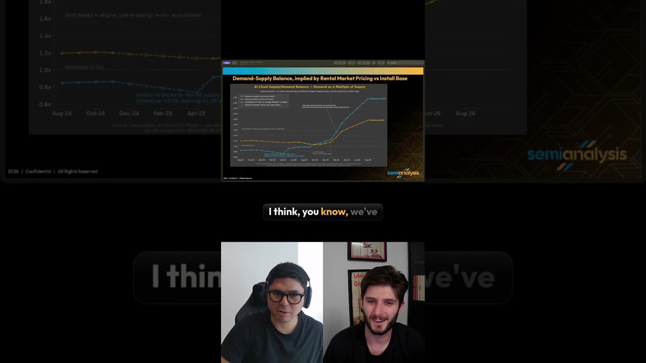




"It's like a zombie apocalypse, but you don't know how many waves of zombies are coming."

Open-source models are already taking the easier tasks. The bull case for frontier labs rests on one

A $200 AI subscription can be worth $12,000 in tokens. Which plan delivers it is not close.
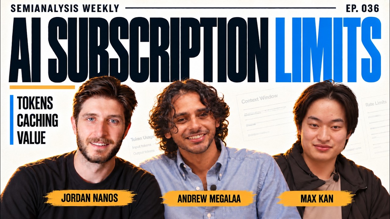
Ep. 036 - Anthropic Subscriptions Beat OpenAI 5x, Depending on Your Workload (Tokenomics)


Ep. 035 - Tech DD’s, Performance Projections, Supply Chain, Investment Thesis (Consulting)
