In this promotional presentation, Dylan Patel (Speaker A) walks viewers through the SemiAnalysis STEEL lab in Hillsboro, Oregon, highlighting its end‑to‑end reverse‑engineering services for both data‑center and consumer hardware. The lab combines expertise from system architecture to device manufacturing, physically tearing down products (racks, consumer boxes) to expose internal components such as displays, chips, advanced packages, interconnects, dies, memory (HBM), and system‑level floor plans. A suite of imaging tools is described: high‑power optical microscopes (micron‑scale), scanning electron microscopes (nanometer‑scale), and transmission electron microscopes (atomic‑scale) that reveal transistors, gates, high‑k dielectrics, and doping layers. The speaker emphasizes the strategic value for technical clients—providing insight into hidden or latent features (e.g., hybrid bonding) to understand competitor differentiation and inform product road‑maps. The talk concludes with a sales contact invitation.
Chapters
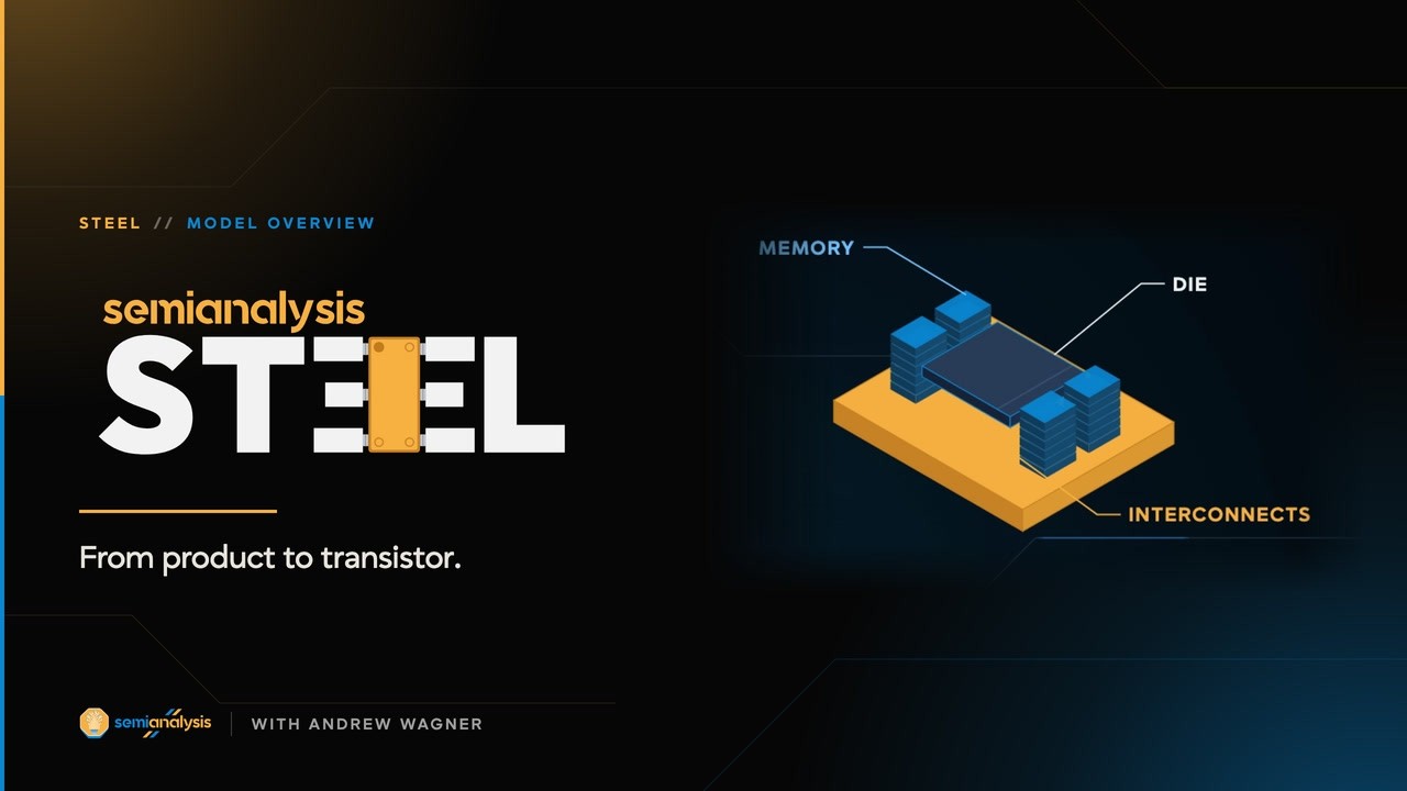
Steel's in Hillsboro, Oregon. That's the center of North America's manufacturing and innovation for all foundry-based manufacturing. And so we're right in the thick of it. We have a lot of experts from system architecture down to device and in manufacturing and process. Tear it down, literally, physically. We get a product in. Data center might be a rack, consumer might be a box that we go and we get at the store, right? We start pulling it apart, looking at what's inside, you know, whether that displays or chips, down to the packages. Very advanced packaging is everything. But we keep going. We break into the interconnects, the different die, memory, HBM. We go in, we look at the die level, we break that down, look at system architecture and floor plan. Yeah, just basic photography, optical microscopes, right? These are high-power optical microscopes. It allows us to see things, you know, at the board level, at the product level, but all the way down to about a micron. We have electron microscopes. We can actually see down with an SEM, we can see down to a nanometer. Well, what the hell's a nanometer, right? Well, we talk about nanometer technologies and transistors. Now we can see the transistor. with an SEM, that's great, but you can't see all the fine detail. You actually have to go to an instrument called a TEM or transmission electron microscope. It uses much higher energy electrons. It actually shoots these electrons through the sample. You collect that data on the other side, and that's how you can see things like gates and high-k dielectrics and doping layers and things like this. Apple loves to test the waters with latent features and design. So the hybrid bonding, the interconnects in there, it's fun to just go in and see these things that maybe aren't even active in the current product, but we're gonna see them in that next product. That's what our technical clients, that's where they're interested in understanding what's there. Why is it there? What does it mean for themselves? How competitors, different companies differentiate and how can they respond? The companies that are going to differentiate and accelerate and make the difference are looking at this in a very holistic and very technically aggressive way. Reach out, sales@semi-analysis.com. Let's talk.