Nvidia Ada Lovelace Leaked Specifications, Die Sizes, Architecture, Cost, And Performance Analysis
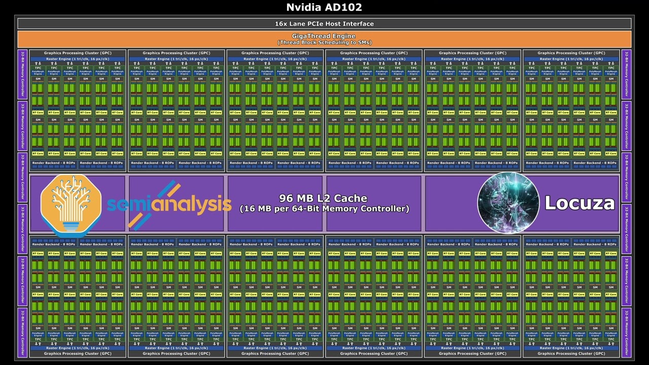
Dylan Patel analyzes Nvidia's leaked Ada Lovelace GPU specs, covering die sizes, architecture changes from Ampere, and cost breakdowns. The top die reaches 611 mm², uses TSMC's custom 4N process, and Ada will deliver the best consumer value in a decade while pushing high-end prices higher.
Chapters
Howdy ho, this is Dylan with SemiAnalysis, and I'm here to bring you some interesting and new information on Nvidia's Ada Lovelace, including some of the leaked specifications, some die sizes, architecture, and cost analysis. Nvidia was the victim of a cyberattack at the end of February where they were hacked for a vast sum of data. This hack was not only a disaster for Nvidia but all chip companies and the national security of All Western countries. Among the hacked data was detailed specifications and simulation data for Nvidia's next-generation GPUs, Hopper and Ada. Hopper is now sampling and was unveiled by Nvidia at GTC. The specs of Hopper match exactly to this leak. But Ada, which is named after the famous computer scientist and mathematician Ada Lovelace, is still many months away from launch. As such, these specifications are very interesting. Based on these leaked specifications and simulations, SemiAnalysis and Lacuza have teamed up to analyze the architecture, die sizes, and do a cost analysis even, as well as product positioning. We did not download any of the leaked files from the Lapsus$ hack. However, many people online shared excerpts, which is what these are based upon. We were able to determine that these were the specs based upon these leaked specs, and they are quite interesting. Here is a table comparing Ampere and Ada Lovelace, the specifications of both. The rest of this video will go through and talk about the block diagrams of each chip, the architecture, and an estimated die size. We're also going to explain how we arrived at this die size. Given both Lacuza and SemiAnalysis are directly supported by our subscribers, we would greatly appreciate it if you could read the, you know, watch the rest of this video, subscribe to my free or paid newsletter, and subscribe to Lacuza on Patreon. So starting off, the top dog in the Ada Lovelace architecture is the AD102 die, and we have estimated it to be 611.3 millimeters squared. It's a huge jump over the previous generation GA102 in terms of performance, right? We've got 70% more CUDA cores coming from 5 additional GPCs. The memory bus width remains at 384-bit bus though, so we can expect memory speeds to improve slightly to somewhere in the region of 21 gigabytes per second, maybe a little bit higher. Uh, but mostly around there. So, so this increase in memory bandwidth is not enough to feed the beast that is Ada Lovelace 102. As such, NVIDIA seems to have added 96 megabytes of L2 cache, which is way larger than Ampere's GA102's 6 megabytes of L2 cache. Now we can use this and, and point and look at AMD's Navi 22 GPU. And AMD's Navi RDNA 2 GPU architecture has a feature called Infinity Cache, which is a large L3 cache. We hope Nvidia names their large L2 Infinity Cache just as a troll, but yeah, that's probably not going to happen. The marketing folks probably have a better idea. But based on this, we can see that there's a difference in cache hierarchy between the 2 vendors. But we expect the general trend of hit rates to be largely the same. As such, AMD has hit rates of 78% at 1080p, 69% at 1440p, and 53% in 4K. So these hit rates are basically when you don't need to go to memory in the process of rendering something. And so they reduce the memory bandwidth requirements. NVIDIA's L2 work should work largely in the same manner and will help feed AD102 despite the small increase in memory bandwidth. The top-end configuration of AD102 should probably be 24GB of GDDR6X for the gaming market, but we expect it to be cut down from this further. The next GPU in the lineup would be AD103. AD103 is quite interesting as a configuration, and we've estimated it at 379 0.69 millimeters squared versus AD102. It is a huge downgrade. This may be the largest gap between the top die and the second die in a GPU generation, with AD102 having more than 70% CUDA cores versus AD103. The other interesting thing is that the CUDA cores are the exact same as the current generation GA102. Despite this, the memory bus comes in at 256-bit, so this is the exact same as GA104 in the current generation Ampere. So with a much smaller memory bus than AD102 at 384, um, this, this means that gaming GPUs based on AD103 would max out probably at 16GB, but cut-down variants will likely exist. Despite memory bandwidth being much lower than GA102, the inclusion of 64 megabytes of L2 cache should probably allow this GPU to be fed. Given Nvidia is utilizing a custom TSMC 4N node, which is a variant of TSMC's N4 or N4P, we expect that they will be able to clock much higher than GA102. The increase in clocks combined with some of the architectural enhancements that we expect Well, which we'll get to later in this video, will allow 8103 to perform better than the current generation flagship RTX 3090 Ti if they bring it— that is, if they bring it to the desktop with a high amount of power consumption. It's important to note that GA103 never came to desktop and is really only available in the top end of laptop GPUs, so this could happen again with the Ada generation. AD104 is estimated at 300 millimeter— 300.45 millimeters squared. This is the sweet spot for Ada. It's— this is due to its performance and cost-effectiveness. The GPU is quite small, which is nice, and it also only has a 192-megabyte bit bus, uh, 192-bit bus, which would lead to it having 12 gigabytes of memory for the gaming GPU market, which is high enough capacity for current use cases and developing games, but— or newer games, but it also keeps the bill of materials, the BOM, down to a reasonable level, right? If you go to 16 gigabytes, that would just be too costly. Simultaneously, Nvidia GPUs tend to have their 104 designs have similar performance to the prior 102. If this trend keeps up, The cost to performance would be excellent. In fact, it may even have more performance than the current generation GA102, given Nvidia is likely to pump clocks quite a bit to hit performance above the 3090. We expect Nvidia to go as high as 350W or maybe even 400W for AD104 desktop GPU with GDDR6X. As such, we expect this GPU to be the one that most enthusiasts end up purchasing because it's still within a reasonable price range. The GPU will also be highly efficient, right? You know, with G6X, you know, that's— there is some inefficiencies, but when we move down to the laptop world, it can be very efficient if you, you know, clock it to the right levels and keep it with regular G6 memory at, you know, 14 or 16 gigabit a second, and the total power consumption, you know, around the 90 to 135 watt. AD106 is the true mass-market GPU of this generation. It's estimated at a tiny 203.21 millimeters squared. It's likely going to be the highest volume GPU in the lineup, as the 106 GPUs are always the highest end. At least they were for Pascal, Turing, and Ampere. Due to the tiny 128-bit bus you know, the memory will most likely max out at 8GB. In the top configuration, we expect it to perform very similarly to GA104's 3070. It might even beat the 3070 and get up to 3070 Ti levels. That assumption might be optimistic given there's only 3 GPCs in AD106 versus the 6 in GA104, but Nvidia might be able to solve this, you know, with higher clocks and with— their large 32 megabytes of L2 cache. You know, with those hot 32 megabytes of L2 cache, the GPU cache rates are going to be 55%— hit rates for their cache is going to be 55% in 1080p, 38% in 1440p, and 27% in 4K. Uh, so this would, this would match, you know, this is based on AMD's Navi 23, which also has a similarly sized 32 megabytes of L2 cache. So before we move on to the, you know, the baby of the generation, AD107, we want to give a bit of background. The data posted on Twitter from the leaked files does not specify a cache size for this GPU. The prior GPUs in this lineup had a 16-megabyte, you know, L2 cache per 64 bits of memory controller or frame buffer partition. With that, that would mean AD107 wouldn't make much sense because the GPC count and the bus width are identical. And the TPCs per GPU only fell by 4. So if the L2 cache stays the same, you know, with that same 16 megabytes per 64 bits of memory controller or FBP, then the die size would only fall to 203 millimeters squared, um, from 203 to 184.28 millimeters squared. This is a tiny decrease and would not be enough to separate the 2 GPUs in the stack. Instead, you know, we can, we can look back at Turing. And Turing actually had an interesting phenomenon where TU106 and TU116 had a similar relationship, right? Where, you know, Nvidia, Nvidia pulled a couple things, different things out of this, right? They made the bus width slightly smaller, yes, and they pulled ray tracing and Tensor Cores out. But, you know, one of the things that people often overlook is that they also reduced the amount of cache per FBP. They went with 0.5 megabytes or 512 kilobytes of L2 cache instead of 1 megabyte as the rest of the Turing, you know, the higher-end Turing lineup did. And so if we apply that same pattern of half the L2 cache per FBP, then AD107 ends up being around 145.54 millimeters squared. So that's a much more reasonable die size. And it would make sense given, you know, product positioning and and cost and, you know, having to hit every point in the market for this. So moving on to GA— to AD107, you know, they're also going to cut down the PCIe lanes to 8x, um, and, you know, cut down the cache and cut down the core count slightly. Um, as such, you know, you know, they, they always cut down this 107 die to 8 lanes because more are unneeded. Um, there's no need to have 16x, and plus this, this bottom GPU is generally in the mobile world anyways, where 8x makes more sense from power perspective as well. So this GPU would still blow the socks off of Intel's Meteor Lake integrated graphics or even AMD's RDNA 2-based Rembrandt or even their Phoenix, next-generation Phoenix APU. So this would still be cheap at such a small die size of 145.54 millimeters squared, but it would also be faster than any integrated graphics. So it would make sense in some of these lower-cost laptops that still want— where the buyers still want to game. Overall, Ada is quite an interesting lineup. At the top end, there's quite the increase in performance and probably power consumption. And AD102 is a similar die size to GA102. But this is on a much more expensive, customized TSMC 4nm process node rather than the very cheap Customized Samsung 8N process node. The density increase from a TSMC N4 derivative is quite large relative to Samsung's you know 8 nanometer derivatives, which would justify the cost increase per wafer. But you know likewise, you know despite being a much newer node, TSMC N4 actually has better parametric yield than Samsung's 8 nanometer despite you know similar catastrophic catastrophic yields. So catastrophic yields are when a feature within the silicon die does not function. Parametric yield is, yes, it functions, but it functions at the level we want it to. The issue with Samsung's nodes is often not defects, catastrophic yields, but parametric yields in that they do not— they can get the transistors to work, but oh crap, this transistor's really bad, or this area of the die is very bad, and it causes the entire chip to have to have much lower clocks. So, you know, this parametric yield, um, being higher is, is, you know, very important as, you know, GPUs are a very yield-harvestable design and very large dies. So, you know, they can keep more parts of the die enabled, you know, which is something that we've seen on GA104 where, you know, a lot of, a lot of the die was disabled in the case of something like a 3080, um, and a 3060 Ti even. So the rest of Ada comes away a lot tamer than AD102 in terms of die sizes and overall bill of materials cost to manufacture. Performance should generally be above that of Ampere's at the same power, which is with a decently lower cost to fabricate despite the much higher wafer costs of TSMC's 4 process node. We played around with the wafer costs and die calculations, and we came up with some estimations, and we even included some Various costs related to passives such as VRMs and other active components like the memory. And in the end, the prices shouldn't be too bad. I think consumers will actually win with this generation. Nvidia sells the die with a markup, right? Everyone knows that. And then they negotiate a bulk memory pricing for original device manufacturers and add-in-board partners to use. So these add-in-board partners still buy the die from NVIDIA, and then they buy the memory, which already has a negotiated price from the vendors of memory, and they integrate that alongside all the power components and cooling and et cetera. So the die cost has a different effect dollar for dollar, how much more a die costs versus how much more memory or VRMs cost. And so NVIDIA seems to have balanced their L2 caches with the memory size and memory bus width optimally, right? You don't want to go too wide on the memory bus or too narrow because then that's going to influence your memory capacities on these GPUs. Memory sizes seem to stay very reasonable, and most GPUs will probably have 16-gigabit dies of G6X or G6. Um, in, in general, AD104 is going to be replacing GA102 in terms of performance, you know, actually beating it some while also costing less. While AD106 is going to replace, you know, the current GA104-based dies in the performance tier, right? So 3070s, think of that, that level. Uh, and so in, in, when you, when you think about it from that perspective, the memory cost is identical, right? Because AD104 should have similar memory sizes to GA102, and AD106 will have similar memory sizes to GA104, AD106 to GA104. You know, they will move from 8 gigabit to 16 gigabit, but the cost to fab the die is actually going to be less despite the more expensive node because of a much larger, you know, much, much smaller die. Board components such as packaging, cooling, power components are actually going to end up being cheaper, generally due to the better efficiency, lower power consumption, and smaller boards that these GPUs will require. So, you know, when we compare dies in the stack, you know, GA104 versus AD104, there is going to be a memory size increase and there's going to be a slight price increase in base MSRP. But, you know, the issue with that is GA104 is only 8 gigabytes, right? Or you can go, you can go with 16-gigabit dies or double-sided and get 16 gigabytes of memory, but then you end up with it being too expensive. So, you know, You know, GA104 is really not in a sweet spot nowadays for memory because of this issue with the bus width, whereas AD104, you know, moves up to 12 gigabit— 12 gigabytes due to their 192-bit bus. Fears of higher power consumption should definitely be taken into consideration. Nvidia is likely pumping power for each die similar to what they did the prior generation. In fact, we imagine that they're going to push power to what one die higher in the stack did. So by that, we mean AD104 will likely reach 3080 levels of power consumption, and AD106 likely reaches 3070 levels of power consumption. And rumors point to the top AD102 breaking records for power consumption. So next, we'll talk about how we arrived at these die size estimates. The first step in the die size analysis was to gather architectural changes regarding Ada and comparing them to Ampere. So the SM architecture is 8.9 versus 8.6 on Ampere. So this is an improvement, but it's a generational improvement. It's not, you know, a whole new SM architecture. As a result, we can assume that the SM die size increased, you know, SM area for an SM increased about 10%. And while we aren't sure what these SM architectural changes are, they likely could be, you know, something like a 192-bit kilobit L1 cache or new Tensor Cores. The highest probability change in our minds is actually the addition of a new 3rd-generation ray tracing core. You know, other architectural changes are on the I/O front, right? So the leak indicates that NVLink has been removed entirely from the lineup. Which indicates NVIDIA is not going to push the Ada lineup for multi-GPU sort of data center and professional visualization applications, right? There's, you know, the RTX A6000, which can do multiple GPUs and be used for these professional visualization and even data center applications. But that's not going to be possible with Ada, where the 102 die looks like it doesn't have any NVLink. We expect PCIe 5.0 and a better memory controller for the slightly higher-speed GDDR6X, and also DisplayPort 2.0, you know, all these changes to be included. There's also the high likelihood that NVENC and NVDEC, you know, the encoding engine and decoding engine, are upgraded to include, you know, AV1 and, you know, some more feature levels around that. The biggest change with Ada is of course the L2 cache, at least on an area perspective. Instead of the small L2 cache, you know, NVIDIA's taken a picture out of AMD's Infinity Cache book and used a much larger cache across the board. Given we have most of the specifications, architectural changes, and configurations for the lineup, we can actually use Ampere's GA102 IP blocks to recreate a hypothetical GPU with the same specifications as AD102 on Samsung's 8nm. So this would be using, you know, the exact same cache sizes, GPC sizes, memory controller sizes, etc., as GA102. And, you know, we would get— we arrived at a die size of 1,629.6 millimeters squared. That's if Lovelace AD102 had the same architecture and configuration on Samsung's 8-nanometer. This doesn't contemplate the changes in SM architecture, the larger encoder-decoder blocks, PCIe 5.0, DisplayPort 2.0, or a tweaked memory controller and of these other changes, you know, the larger— but it does contemplate, you know, using the same configuration. With this die size of 1,629.6 mm², you can immediately notice that the L2 cache is titanic, right? This is huge. This is larger than, you know, AMD has their large L3 Infinity Cache on Navi 21, but they don't allocate such a large area dedicated to the cache. And yes, while AMD is using a denser TSMC N7 node, this is only a small part of the puzzle. Actually, most of the difference in density comes from a difference in layout and configuration of that cache. So GA102 uses 48 128-kilobyte slices of SRAM with, with a 1-megabyte, you know, L2 cache per 64 bits of memory controller or frame buffer partition. If we look at other places in NVIDIA's lineup, you know, GA100, that uses 80 512-kilobyte slices. So these larger slices have vastly improved density, you know, as seen with the comparison to AMD's L2 cache. The density increase of GA100 is far more than that, just that of the, you know, process node shrink. And yes, while AMD is not as good as NVIDIA in many elements of design, they are undoubtedly better in areas of cache and packaging. We believe a lot of this stems from their CPU teams and the pedigree there. So AMD is very, very good at making extremely dense, high-performance caches, and they applied this to their GPUs with Infinity Cache. In fact, in our final die size estimates, Nvidia's 96 megabytes of L2 is still not as dense as AMD's 96 megabytes of L3 Infinity Cache. And, you know, so regardless of the shrink from Samsung's 8 to TSMC 4, that alone wouldn't make GA102's building blocks reach a reasonable die size. Instead, there is an architectural rework from the ground up required for the cache design. The leaks indicate there is now 16 megabytes of L2 per 64 megabytes of FBP, which is, you know, very different from GA102's 1. And so we estimate Nvidia is going to actually use 48 2,048 kilobyte slices, so 48 2-megabyte slices of SRAM for their L2 cache. rather than 48 128 kilobytes. So a huge increase in, you know, size slice, uh, size, which would greatly increase density. You know, with this cache configuration, we can actually even calculate the theoretical cache bandwidth, uh, with these figures. So AMD has 1.99 terabytes a second of Infinity Cache bandwidth on their Navi 21 GPU when it's clocked at 1.94 gigahertz. If we assume NVIDIA's running at the same, you know, 1.94 GHz on AD102, they would actually be able to achieve 5.96 terabytes a second of bandwidth with their L2. So clocks will differ in the end products, but we expect clocks for Lovelace to, you know, Ada Lovelace to be somewhere around 2.25 GHz, which would be realistic in a desktop platform, right? Whereas with RDNA 2, you know, it can clock higher than, you know, the clock speeds that we indicated before. And in fact, RDNA 3 probably on desktop goes above 2.5 GHz. How much? We're not sure, but most likely it goes above that figure. NVIDIA has, you know, always made the design choice of density over clock speeds, whereas AMD's designs tend to be a little bit more relaxed in comparison. But that doesn't apply to the cache, actually. Nvidia could have introduced a higher density, 8 or 16 megabytes per slice, but then they would have to reduce the number of slices vastly, which would reduce the bandwidth, which isn't tenable given the way L2 works on AMD's architecture with the delta color compression and other aspects. We came up with estimates for what this different cache architecture would do to the area of AD102, you know, using the GA102 building blocks. And so once we accounted for the architectural changes, we also applied shrink factors to TSMC's N7 node and then another one to TSMC's N4 node. And, you know, these shrink factors are not homogeneous across the die, right? Analog shrinks differently than SRAM, which shrinks differently than logic. So the SRAM appears to be about a 60/40 split of SRAM to logic. which influences the SRAM shrink figure that we used. That's for the L2 cache. And then for the rest of the die, we applied a 10% gross-up factor to the SMs to account for any architectural changes there. And we also had some different shrink factors with the various pieces of digital logic because their mix of SRAM to logic was different. The SRAM percentage on these other pieces of logic was generally around 30% and 70% logic. So this made the shrink factor higher. Lastly, we kept the analog portions of the die identical. You know, there is a small shrink, you know, from, from, you know, Samsung's 8 to 7, TSMC 7 to TSMC 4, but it's not that large. And these would probably most likely be equalized with any potential upgrade to PCIe 5.0, a slightly better, you know, GDDR6 memory controller and PHY, and DisplayPort 2.0. So You know, the analog portions we kept pretty much identical. Obviously NVLink was still removed, and that's how we arrived at 611.3 millimeters squared. And actually, that, that, you know, nicely lines up with, you know, what Kopite7Kimi, the famous NVIDIA leaker, has stated. You know, he stated the die size was around 600 millimeters squared. You know, us getting 611.3 seems pretty, pretty, pretty good, and it helps us feel confident in our estimate. So after gathering, you know, this small overview, we could use the configurations for the rest of the lineup, right? GPCs, TPC counts, L2 sizes, you know, the command buffers, the various differences in PHYs, whether it's bus width or PCIe size, you know, display controllers, you know, the crossbar sizes. All of these can be dynamically scaled based upon the GPU configuration. And so, you know, these shrink factor figures can be used That we determined based on some statements from TSMC plus what we've measured in real products. And in the end, it is a bit of a shot in the dark. We're not going to lie to you, but we think it's an educated guess onto the die sizes. For AD107, we will note that we backed off on the architectural shrink due to the smaller amount of cache per FBP, frame buffer partition. So the density gains from larger L2 cache slices do back off slightly at AD107 in our estimate. Overall, Ada Lovelace isn't a massive departure architecturally from the current Ampere architecture, but the changes it brings, such as improved ray tracing cores, improved encoders for AV1, larger L2 cache, these changes bring performance up considerably. But they also keep costs down despite being on the expensive, you know, more expensive custom TSMC N4 node. Nvidia is keeping in— is keeping with the tradition of keeping memory sizes well-balanced across the stack with a moderate increase in memory size per level. Right. They're not going to, you know, too large of memory sizes, which would influence the cost of manufacture and essentially the cost to the end consumer. Instead, they're keeping it modest and they're balancing the size of their L2 with that memory bus width. So that's a good thing to point out versus AMD. Rumors point to very high performance, but also very high cost at the top end of the stack due to this hybrid bonding that they want to introduce, allegedly. But we're much more interested in Navi 33 as a chip, which we assume that it will fall somewhere in between AD104 and AD106, probably closer to AD104. But the range is large because, you know, we don't know the exact, you know, architectural changes. But leaks point to it being a very good competitor in the mass market segment. And, you know, while AMD is currently massively behind in gaming performance in, you know, current or next generation games, depending on how you want to see it, due to their, you know, lackluster ray tracing performance, And, you know, they lack many differentiated software features such as DLSS and RTX Studio, and those hurt competitiveness. But, you know, Navi 33 is going to make this the most competitive GPU generation in a decade. You know, Nvidia is— the reason they're pumping clocks is partially because they want to optimize cost and performance and maximize their margins and performance that the end consumer gets, but also because they're you know, frankly scared of what AMD is going to produce. Um, and so, you know, with GPU prices falling fast as Ethereum 2.0 slams on the brakes from mining demand, you know, the, you know, fall, you know, the slight fall in, you know, the crypto market has caused, you know, mining to become a little bit less profitable. And then, you know, consumers are shifting their spending away from a mix of, you know, goods more towards services. You know, all of these things combined with higher inflation across the whole broader market mean that demand has gone down and prices are coming more in line. And as such, we predict Ada Lovelace and RDNA 3 GPU prices, at least for Navi 33, to be quite good in the price-to-performance market of $400 to $1,000. You know, there'll be a couple of GPUs scattered through there and the top, you know, the top end of the stack will be well above $1,000. Right. Both Nvidia and AMD are going to increase prices on the top of the stack, but, you know, which is great for, you know, you know, the, you know, hyper enthusiasts. But, you know, even for normal people that can't afford, you know, such an expensive GPU, I think this is going to be the best generation for consumers in a long time, right? Much better than, you know, the short-lived Ampere, or much better than Turing, much better than Ampere, right? You know, so, so, um, you know, the short-lived Ampere in the sense that prices skyrocketed a bit after release. But in short, you know, price to performance is gonna go up. And at the top of the stack, cost will, but so will performance move up considerably and consumers will win. So thanks for watching and please subscribe to the channel, to my free or paid newsletter and to Lacuza's Patreon. Thanks, bye. Bye.
More from Dylan




"It's like a zombie apocalypse, but you don't know how many waves of zombies are coming."

Open-source models are already taking the easier tasks. The bull case for frontier labs rests on one

A $200 AI subscription can be worth $12,000 in tokens. Which plan delivers it is not close.

Ep. 036 - Anthropic Subscriptions Beat OpenAI 5x, Depending on Your Workload (Tokenomics)


Ep. 035 - Tech DD’s, Performance Projections, Supply Chain, Investment Thesis (Consulting)
