ASML is bringing lithography-grade precision to hybrid bonding.
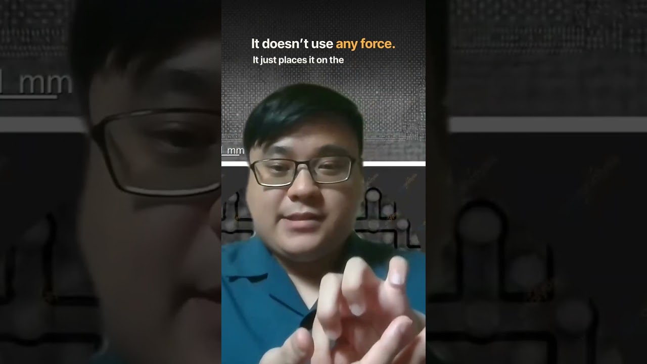
In this video, Dylan Patel discusses the landscape of hybrid bonding equipment, contrasting the established pick‑and‑place solutions from vendors such as Besse and ASMPT with ASML’s novel approach that leverages its front‑end lithography‑grade sub‑nanometer overlay capabilities. The conversation explains how current tools use mechanical arms to position chiplets onto a wafer without applying force, followed by a separate annealing step for bonding. ASML, traditionally a lithography supplier, proposes to bring its ultra‑precise alignment technology directly into the hybrid bonding process, aiming to support ever‑finer bond pitches and higher signal densities. The speakers outline the potential benefits of this front‑end integration, the technical challenges of adapting lithography precision to a die‑to‑wafer or wafer‑to‑die workflow, and the broader implications for future high‑density chiplet integration.
Chapters
More from Dylan


Ep. 040 - ASML Is Building a Hybrid Bonding Tool, and We Have the Patents (AI Supply Chain)